






















The race to build more powerful artificial intelligence systems is increasingly being shaped by something less visible than the processors themselves: the technology used to connect chips together.
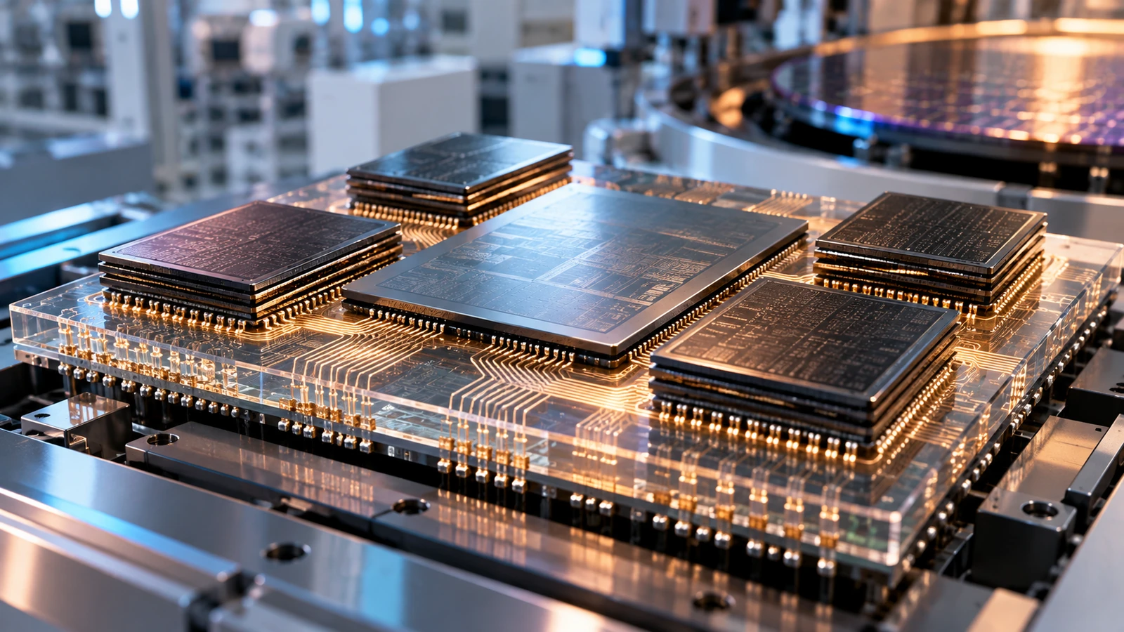
On October 8, 2026, GlobalFoundries announced a $2 billion manufacturing agreement with TSMC to produce silicon interposers at its facility in Malta, New York.
These components are essential to advanced semiconductor packaging because they provide dense, high-speed connections between processors and memory chips.
Under the five-year agreement, GlobalFoundries will expand manufacturing capacity to support TSMC’s Chip-on-Wafer-on-Substrate (CoWoS) advanced packaging ecosystem.
Volume production is expected to begin ramping during the first half of 2028.
The agreement represents a significant development for the semiconductor industry, particularly as demand for AI accelerators continues to increase and advanced packaging capacity becomes an important constraint on production. Reuters
However, the deal does not mean that additional AI processors will immediately become available.
Its importance lies in the longer-term development of manufacturing capacity and supply-chain flexibility.
What Is the GlobalFoundries TSMC Deal?
The GlobalFoundries TSMC deal establishes a manufacturing relationship between two major semiconductor companies.
GlobalFoundries will manufacture silicon interposers that can be used within TSMC’s advanced packaging technologies.
The agreement has an initial duration of five years and is valued at $2 billion.
According to GlobalFoundries’ official announcement, the company will expand fabrication capacity at its existing Malta facility.
The additional manufacturing capability is intended to support multiple generations of advanced semiconductor packages.
The agreement also provides a framework for further expansion as demand develops. GlobalFoundries
The most important details are summarized below.
| Agreement Detail | Confirmed Information |
|---|---|
| Companies | GlobalFoundries and TSMC |
| Announcement | October 8, 2026 |
| Agreement value | $2 billion |
| Initial duration | Five years |
| Manufacturing location | Malta, New York, United States |
| Component | Silicon interposers |
| Target technology | TSMC CoWoS advanced packaging |
| Expected production ramp | First half of 2028 |
| Future expansion | Possible, depending on demand |
Although the financial value is substantial, the companies have not disclosed the planned annual production volume or the precise amount of manufacturing investment required.
The $2 billion figure should therefore not be interpreted as an immediate investment expenditure or annual revenue contribution.
Why Silicon Interposers Are Essential for AI Chips
To understand the importance of the agreement, it is necessary to examine how modern AI processors are constructed.
Traditional semiconductor designs often concentrated major computing functions on a single chip.
Modern high-performance processors increasingly use multiple semiconductor dies, or chiplets, assembled into a larger package.
This architecture allows manufacturers to combine different computing and memory components within a tightly integrated system.
However, connecting those components efficiently is a major engineering challenge.
What Is a Silicon Interposer?
A silicon interposer is a thin semiconductor structure positioned between computing components and the package substrate.
It contains extremely dense electrical connections that allow different chips to communicate.
In an advanced AI processor package, an interposer can connect a central computing die to multiple stacks of high-bandwidth memory.
These connections must support extremely high data-transfer rates while maintaining acceptable power consumption and signal integrity.
An interposer is not itself the primary AI computing engine.
Instead, it provides the physical communication infrastructure that allows the computing and memory components to operate together efficiently.
This makes it a critical part of advanced semiconductor packaging.
Why AI Processors Need High-Bandwidth Memory
Artificial intelligence workloads frequently involve moving large amounts of data between processors and memory.
Training and running sophisticated neural networks requires repeated access to model parameters, intermediate calculations, and other information.
Even an extremely powerful processor can become limited if memory cannot supply data quickly enough.
High-bandwidth memory, commonly known as HBM, addresses this problem by using vertically stacked memory dies and wide interfaces.
Advanced packaging technologies allow HBM stacks to be positioned close to computing processors.
The resulting short, dense electrical connections help support high data-transfer rates.
TSMC identifies the integration of computing chips and HBM as a central capability of its CoWoS platform. 3DFabric
How TSMC’s CoWoS Technology Works
CoWoS stands for Chip-on-Wafer-on-Substrate.
It is an advanced packaging technology designed to integrate multiple semiconductor components within a single package.
The technology is often described as 2.5D packaging because multiple chips are positioned alongside one another on an interconnection structure rather than being integrated exclusively through conventional vertical chip stacking.
TSMC has developed several CoWoS technologies for different requirements.
CoWoS-S: Silicon-Based Interposers
CoWoS-S uses a silicon interposer to provide high-density connections between computing dies and memory components.
This approach supports advanced high-performance computing applications where communication bandwidth and signal integrity are critical.
TSMC states that CoWoS-S can accommodate interposers up to approximately 3.3 times the conventional lithography reticle size.
The technology also supports embedded deep trench capacitors, which help manage power delivery.
CoWoS-R: Redistribution-Layer Interposers
CoWoS-R uses a redistribution-layer interposer rather than relying on a large silicon interposer.
This approach employs conductive routing structures that can offer different scaling and mechanical characteristics.
TSMC says the technology entered volume production in 2023.
CoWoS-L: Local Silicon Interconnects
CoWoS-L combines redistribution-layer technology with localized silicon interconnect structures.
This architecture is intended to support increasingly large and complex high-performance computing packages.
It also allows additional components, including capacitors, to be incorporated into the package.
TSMC reports that CoWoS-L entered volume production in 2024.
These variations demonstrate why advanced packaging has become a specialized semiconductor technology rather than simply the final assembly stage of chip production. 3DFabric
Importantly, GlobalFoundries has not publicly specified which individual CoWoS configurations will use its new interposers.
The agreement identifies the broader CoWoS ecosystem rather than a complete list of supported processor designs.
Why Advanced Packaging Has Become a Semiconductor Bottleneck
The semiconductor industry has traditionally focused heavily on manufacturing smaller transistors.
That remains important, but improvements in transistor density alone are no longer sufficient to deliver every required performance increase.
AI processors need enormous computing capacity, high memory bandwidth, efficient power delivery, and sophisticated communication between components.
Advanced packaging helps address these requirements.
However, producing sophisticated packages requires specialized equipment, manufacturing processes, materials, and engineering expertise.
Expanding production therefore involves more than increasing the number of wafers manufactured at leading-edge semiconductor factories.
Packaging capacity must also grow.
Reuters reported on October 8 that advanced packaging has become a significant constraint on AI chip production because demand exceeds available manufacturing capacity. Reuters
Why Manufacturing More Chips Is Not Enough
Consider a hypothetical AI accelerator containing a computing processor and several HBM stacks.
The computing die may be manufactured successfully.
The memory components may also be available.
But the finished accelerator still cannot be delivered unless those components can be assembled into a functioning package.
If suitable interposers or advanced packaging capacity are unavailable, the completed product can be delayed.
This illustrates why semiconductor manufacturing capacity cannot be measured solely by the number of advanced logic wafers produced.
The entire production chain matters.
Packaging Is Becoming Part of Processor Design
Advanced packaging also influences how chip architects design future processors.
Instead of building every function into one large silicon die, engineers can divide a system into specialized chiplets.
Different chiplets can potentially be manufactured using different process technologies.
For example, high-performance computing logic may require an advanced manufacturing process, while supporting functions may not.
Integrating these components through advanced packaging can provide additional architectural flexibility.
But it also introduces engineering challenges involving thermal management, communication latency, signal integrity, and power delivery.
The package itself is increasingly part of the computing architecture.
Why TSMC Is Working With GlobalFoundries
The partnership is particularly interesting because both companies operate semiconductor foundries.
TSMC is widely associated with manufacturing advanced processors for major technology companies.
GlobalFoundries operates a differentiated semiconductor manufacturing business serving markets including communications, automotive, industrial systems, and data-center infrastructure.
Although their businesses overlap, they do not compete identically across every semiconductor technology.
The new agreement illustrates how specialization can create opportunities for cooperation.
A More Distributed Manufacturing Model
Under the announced arrangement, GlobalFoundries will manufacture a specific component used in TSMC’s packaging ecosystem.
This does not mean GlobalFoundries is taking over TSMC’s complete advanced packaging process.
Nor does it mean the company will manufacture the leading-edge computing dies used in those packages.
Instead, the relationship separates part of the manufacturing process from the broader packaging operation.
Such specialization can allow semiconductor companies to expand supply without duplicating every stage of production.
It can also create additional manufacturing options for future products.
Why the Malta Facility Matters
GlobalFoundries’ Malta site is an established semiconductor manufacturing location in New York.
The company plans to expand capacity there to support the new agreement.
GlobalFoundries describes the project as establishing a U.S.-based source of silicon interposers for TSMC’s advanced packaging ecosystem.
The company also expects the expanded capability to support interposers incorporating embedded deep trench capacitor components. GlobalFoundries
That represents a strategic manufacturing opportunity for the facility.
However, it is important not to interpret the announcement as proof that all silicon interposer manufacturing is moving to the United States.
The deal establishes a particular U.S. supply relationship within a global semiconductor industry.
Why Embedded Deep Trench Capacitors Matter
One technical detail in the announcement deserves particular attention.
GlobalFoundries specifically mentions support for embedded deep trench capacitors, often abbreviated as eDTC.
These components help manage electrical power within advanced semiconductor packages.
Modern AI processors can experience rapid changes in power demand as computing workloads fluctuate.
Those changes can create electrical noise and voltage instability.
Capacitors help stabilize the power supply by storing and releasing electrical charge.
Deep trench capacitors use structures formed within silicon to provide capacitance in a compact area.
Integrating them into an interposer can help improve power delivery close to the computing components.
This becomes increasingly valuable as semiconductor packages incorporate more computing dies, memory stacks, and high-speed connections.
TSMC also identifies embedded deep trench capacitors as an important feature of its advanced packaging technologies. 3DFabric
The inclusion of this capability suggests that the manufacturing agreement concerns technically sophisticated interposers rather than simple mechanical support structures.
Why the Deal Matters for U.S. Semiconductor Manufacturing
The geographic location of semiconductor production has become an important issue for technology companies and governments.
Advanced semiconductor supply chains involve manufacturing facilities distributed across multiple countries.
This creates opportunities for specialization and efficiency.
It also introduces exposure to logistical disruptions, trade restrictions, geopolitical tensions, and manufacturing interruptions.
Adding manufacturing capacity in another location can improve supply-chain flexibility.
The GlobalFoundries TSMC deal is therefore relevant beyond the two companies directly involved.
Strengthening Supply-Chain Resilience
A geographically distributed supply chain can reduce dependence on individual manufacturing locations.
If a particular component can be produced in multiple regions, customers may have more options when disruptions occur.
However, geographic diversification does not automatically eliminate supply-chain risk.
Semiconductor manufacturing still depends on specialized equipment, materials, intellectual property, and international logistics.
A U.S.-manufactured interposer may be combined with processors and memory produced elsewhere.
The resulting semiconductor package may also undergo additional manufacturing and testing stages in other locations.
Consequently, the agreement should not be described as creating a completely domestic AI chip supply chain.
Its confirmed contribution is narrower: adding a planned U.S. manufacturing source for an important advanced packaging component.
What the $2 Billion Agreement Does Not Tell Us
The announcement establishes several important facts, but significant commercial and technical details remain undisclosed.
GlobalFoundries has confirmed the agreement’s value, initial duration, manufacturing location, and expected production-ramp period.
It has not publicly disclosed a detailed annual production target.
The announcement also does not identify specific AI processor models that will use the interposers.
Nor does it establish how much additional CoWoS packaging capacity the project will ultimately enable.
These omissions matter because a manufacturing agreement’s strategic importance cannot be translated directly into a specific increase in chip shipments.
The Difference Between Contract Value and Investment
The $2 billion headline describes the value of the manufacturing agreement.
It should not automatically be interpreted as the amount GlobalFoundries will spend constructing or upgrading facilities.
Similarly, it does not mean the company will recognize $2 billion in revenue immediately.
The agreement covers multiple years, and actual financial outcomes will depend on production, deliveries, contract terms, and other factors.
Those details have not been fully disclosed.
Production Will Not Ramp Until 2028
Another important limitation is timing.
GlobalFoundries expects volume production to begin ramping in the first half of 2028.
That is a future manufacturing milestone, not a statement that the planned capacity is already operating.
The project must still move through capacity expansion, manufacturing preparation, qualification, and production scaling.
The announced timeline therefore suggests a longer-term supply-chain strategy rather than an immediate solution to current shortages.
The company also cautions that its forward-looking plans are subject to risks and uncertainties. GlobalFoundries Inc.
Could the Agreement Make AI Chips Cheaper?
Additional manufacturing capacity can potentially reduce supply constraints.
However, the announcement does not provide enough information to predict future AI accelerator prices.
Semiconductor pricing depends on numerous factors, including manufacturing yields, memory availability, packaging costs, demand, product design, and commercial agreements.
Increasing interposer supply may help relieve one constraint while other constraints remain.
For example, greater packaging capacity will not necessarily resolve shortages of high-bandwidth memory.
Nor will it automatically increase the number of advanced computing dies available.
The relationship between component capacity and finished accelerator pricing is therefore complex.
A more realistic expectation is that additional interposer manufacturing capacity could improve production flexibility over time.
Whether that produces lower prices, shorter delivery times, or higher shipment volumes remains to be demonstrated.
What This Means for AI Developers and Cloud Providers
The agreement will not immediately change how developers use AI models.
There is no new software framework, API, or processor architecture being introduced through the manufacturing announcement.
Its potential impact is further upstream.
AI developers depend on access to computing infrastructure.
Cloud providers depend on acquiring and operating large quantities of advanced processors.
Those processors depend on a complex semiconductor manufacturing ecosystem.
If packaging capacity becomes more widely available, it could eventually support greater production of AI computing hardware.
That, in turn, may influence the availability of cloud computing capacity.
However, such effects would be indirect and depend on multiple stages of the supply chain.
Developers should not assume that this agreement alone will reduce GPU rental prices or improve access to AI accelerators.
The announcement provides evidence of planned manufacturing expansion, not a forecast of cloud computing costs.
What Happens Next?
The next major milestone will be the development of additional manufacturing capacity at GlobalFoundries’ Malta facility.
Several questions will determine the agreement’s long-term significance.
The first is whether the project remains on schedule for its planned production ramp in the first half of 2028.
The second is how much manufacturing capacity the expansion ultimately provides.
The third is which generations of advanced packaging technology will use the new interposers.
Another important question is whether TSMC and GlobalFoundries expand the relationship beyond the initial five-year agreement.
GlobalFoundries has already indicated that the arrangement provides a framework for future capacity expansion.
That possibility should be treated as an option rather than a confirmed commitment to additional production.
Frequently Asked Questions
What is the GlobalFoundries TSMC deal?
It is a five-year manufacturing agreement valued at $2 billion. GlobalFoundries will manufacture silicon interposers in New York for TSMC’s advanced packaging ecosystem.
What is a silicon interposer?
A silicon interposer is a semiconductor structure that provides dense electrical connections between components such as computing processors and high-bandwidth memory.
Where will the components be manufactured?
GlobalFoundries plans to manufacture the interposers at its facility in Malta, New York.
When will production begin?
The company expects volume production to begin ramping during the first half of 2028.
What is TSMC CoWoS?
CoWoS is an advanced semiconductor packaging technology that integrates computing dies and memory components within a single package.
Will this agreement solve AI chip shortages?
Not immediately. The agreement is intended to expand future manufacturing capacity, but it does not establish how much additional AI hardware will become available.
Does GlobalFoundries manufacture the AI processors themselves under this agreement?
No. The announced manufacturing arrangement specifically concerns silicon interposers used in advanced packaging.
Conclusion: AI Hardware Depends on More Than Advanced Processors
The GlobalFoundries TSMC deal highlights an increasingly important reality of semiconductor technology.
Building more powerful AI systems requires more than developing faster processors.
Manufacturers must also provide the memory, interconnections, power-delivery components, and packaging technologies needed to assemble those processors into functioning systems.
The $2 billion agreement addresses one part of that challenge.
By establishing additional U.S. manufacturing capacity for silicon interposers, GlobalFoundries and TSMC aim to strengthen the infrastructure supporting future generations of AI hardware.
The project also illustrates how semiconductor companies can cooperate across specialized manufacturing processes even when they compete in other markets.
Its immediate impact should not be overstated.
Production is not expected to ramp until 2028, and important details about capacity, customers, and financial outcomes remain undisclosed.
Nevertheless, the agreement demonstrates why advanced packaging is becoming a strategic part of the semiconductor industry.
As artificial intelligence workloads grow more demanding, the ability to connect processors and memory efficiently may become just as important as improvements in the computing chips themselves.

TechnologyHQ is a platform about business insights, tech, 4IR, digital transformation, AI, Blockchain, Cybersecurity, and social media for businesses.
We manage social media groups with more than 200,000 members with almost 100% engagement.