


 in the World of Online Casinos")


")
")


With the accelerated deployment of 10Gbps fiber-to-the-home technology in the access network, the market demand for 10G small-package optical transceiver modules has increased. At the same time, the competition in the optical communication market has become more and more fierce, and the cost control of optical modules has become more stringent. The production cost of “independent chip assembly” in the industry is relatively high, and improvement and optimization are carried out by independently designing circuits and software, thereby reducing production costs.
This paper verifies for the first time that the 10G SFP+ SR optical transceiver module circuit adopts a single chip integrated with laser driver, limiting amplifier, controller and clock recovery unit. On the basis of ensuring high-precision digital diagnosis function, it achieves the characteristics of low cost and high reliability.
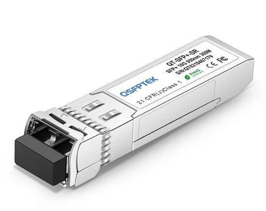
What is 10G SFP+ SR Optical Transceiver Module?
SFP+ Optical Transceiver Module (10 Gigabit Small Form Factor Pluggable) is a hot-pluggable, communication protocol-independent optical transceiver. 10G SFP+ SR transmits light at a wavelength of 850nm, which can transmit 300m on OM3 and 300m on OM4. It can transmit 400m. It is used in applications such as 10 Gbps SONET/SDH, Fibre Channel, gigabit Ethernet and 10 gigabit Ethernet.
Most of the electronic signal processing in the 10G SFP+ SR optical transceiver module is done on the motherboard rather than inside the module. We design the SFP+ 10Gbps serial electrical interface according to SFF-8472 requirements. This interface uses the integrated transceiver on the printed circuit board with electronic signal processing function, the transceiver ASIC is placed on the PCB printed circuit board, and the 10Gbps serial interface is implemented on the traditional FR4 printed circuit board to ensure that the interface is traversing 8~12. inch printed circuit board interconnects still provide adequate signal amplitude and fidelity. In this paper, Ansoft Designer simulation software is used to design the SFP+ module with digital diagnosis function, which shows that the use of simulation software and the actual processing of the SFP+ module has certain guiding significance, which can speed up the design process of the optical transceiver module.
Low-cost 10G SFP+ SR Optical Transceiver Module Circuit Design
SFI is a differential signal serial interconnection line with two specifications. Currently, SFI-4 is the most used, which supports 10Gb/s data bandwidth. SFI-4 is divided into a receiver and a transmitter, which is point-to-point communication with a nominal baud rate of 9.95 to 10.75Gbps. A typical end-to-end electrical channel for an SFP+ application part includes a transceiver circuit pack within an SFP+ module, which can be simulated, packaged in a 10Gbps channel simulation. Simulating and measuring this electrical channel can guide the SFI design.
In the case of the evaluation board stack, the total board thickness is 36mil, the board material is standard FR4 with εr=4 and loss tangent 0.016. In the receiving direction, first adjust the phase relationship between the data and the clock so that the rising edge of the clock is in the middle of the valid data window; in the sending direction, according to the phase requirements of the docking chip, the clock edge is sent to align with the data edge in the same direction. This is the SFI-4 principle. It is worth noting that all information of the SFI-4 protocol is in the data edges with the clock edges aligned in the same direction. In the application, the data and clock are source synchronous and edge-aligned. Figure 3 shows the case where the rising edge of the clock is aligned with the sending and receiving data edges.
QSFPTEK 10G SFP+ SR
Optical transceiver module circuit board structure, the most prominent feature is that the transmitted signal will be attenuated when passing through the printed circuit board. When transmitting signals at 10Gbps, the main defect of the FR4 dielectric substrate in the PCB is dielectric loss. Differential transmission line losses on FR4 substrates are 0.5dB/inch and 0.9dB/inch at 10GHz.
This loss low-pass filters the transmitted digital signal. Therefore, it limits the distance that an uncompensated 10 Gbps signal can travel on a printed circuit board transmission line. The signal conditioning circuit inside the 10G SFP+ SR module can compensate for this filtering and enable transmission distances up to 12 inches. The challenge for the PCB is to provide transmission lines with appropriate characteristic impedance and routing and via designs with sufficiently low return loss.
This article verifies that QSFPTEK’s low-cost 10G SFP+ SR optical module circuit has good reliability. Welcome to contact [email protected] for bulk quotations.
TechnologyHQ is a platform about business insights, tech, 4IR, digital transformation, AI, Blockchain, Cybersecurity, and social media for businesses.
We manage social media groups with more than 200,000 members with almost 100% engagement.


 in the World of Online Casinos")


